|

|
VACCARO Pablo O. Adaptive Communications Research Laboratories |
|
We are researching a whole family of opto-electronic devices based on the original concept of lateral p-n junctions. Lateral p-n junctions have particular properties and are promising for applications in opto-electronic integrated circuits. We fabricated light-emitting diodes (LEDs), vertical-cavity surface-emitting lasers and photodiodes using lateral p-n junctions, and demonstrated high-density integration in LED arrays. 1. Introduction |
||
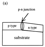 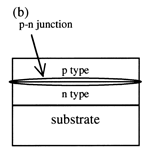 Fig. 1. (a) Lateral p-n junction and (b) conventional p-n junction. |
Lateral p-n junctions thus prepared are promising as next-generation devices because they have the following advantages.
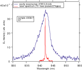
We proposed and demonstrated various devices that use these advantageous properties of lateral junctions and fabricated high-density linear arrays of light emitting diodes (LEDs). In this article, we introduce these devices. 2. Lateral junction devices 2-2 Lasers |
|
2-3 Photodetectors
For optical wireless communication systems, photodetectors, which detect light, are important devices. To make the system faster, we need photodetectors with a faster response, which can be accomplished by the reduction of the capacitance of the devices. Fast operation of lateral-junction photodetectors was demonstrated, taking advantage of the small junction area of the LJ devices, which led to small capacitance of the devices [4]. 3. Array of lateral junction LEDs |
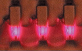 Fig. 3. Optical micrograph of the light emission from the array of lateral junction LEDs with a 2400-dpi density. |
4. Conclusion
We will develop opto-electronic devices for optical wireless communication systems with higher performance using lateral p-n junctions, which have many advantages. References [1] H. Ohnishi, M. Hirai, K. Fujita and T. Watanabe, "Lateral tunneling devices on GaAs (111)A and (311)A patterned substrates grown by MBE using only silicon dopant", Jpn. J. Appl. Phys. 35, 1168 (1996). |