|

|
SAITO Nobuo Adaptive Communications Research Laboratories |
|
This report looks at the present and future of research on opto-electronic devices aiming to create next-generation devices based on ATR's research activities in the field of compound semiconductor technology. The results introduced in previous articles, the 2-dimensional microcavity laser, Micro-origami, and lateral junctions, are all made of compound semiconductors, and are expected to be developed into small-sized high-performance opto-electronic devices by integration. 1. Introduction |
||
Table I: Typical elements in columns III, IV, and V |
elements in I column II |
elements in column IV |
elements in column V |
boron (B) |
carbon (c) |
nitrogen (N) |
aluminum (Al) |
silicon (Si) |
phosphorus (P) |
gallium (Ga) |
germanium (Ge) |
arsenic (As) |
indium (In) |
tin (Sn) |
antimony (Sb) |
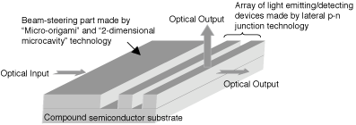
2. Advantages of compound semiconductors 3. Next-generation opto-electronic devices by integration of beam-steering devices and light emitting/detecting devices Although this kind of device has already been proposed, they are mainly made of Si. Manufacturing technology for Si is highly sophisticated, and a lot of high-performance devices and systems have been demonstrated [1]. However, most of these devices required the assembling of many parts, mainly due to the difficulty in fabricating light emitting devices using Si. On the other hand, if we use the compound semiconductor technology developed here at ATR, it becomes possible to fabricate integrated opto-electronic devices, which is the integration of light emitting/detecting devices and beam-steering devices. Since we might be able to achieve compact opto-electronic devices, which can control many beams with a high speed, by making use of our compound semiconductor technology, we expect that they will lead to next-generation devices. |
|
4. Aiming at eye-safe light sources
In optical wireless communication, the light that is used must be completely safe for human eyes, so that no harm is done even if the light gets into the eyes. Lasers that meet this requirement are called eye-safe lasers, key devices in optical wireless communication. We can obtain lasers that shine in the infrared wavelength region by using a compound semiconductor, as is mentioned in this article. This is another advantage of the compound semiconductor. We are conducting research to create eye-safe lasers making use of the phenomenon that the emission wavelength of InAs, a kind of III-V compound semiconductor, changes according to the size when it is made as small as several tens of nm in diameter (quantum dots). We are trying to solve the problem that the light intensity becomes small as the wavelength becomes long by improving the film structure. Our recent results are shown in Figure 2 [2] . In the future, we are planning to combine eye-safe optical devices with the next-generation opto-electronic devices discussed in Section 3. Such a fruitful combination of technologies is made possible by the fact that all of these devices are based on the same III-V compound semiconductor. |
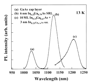 Fig. 2. Photoluminescence spectrum of the materials for eye-safe lasers. |
5. Conclusion
We introduced our research aiming towards integrated devices of light emitting devices, which operate in wavelength regions that are safe to the human eye, photodetectors, and beam-steering devices. We must also make individual devices smaller to improve the degree of integration. To meet this requirement, we have begun research on a fine manufacturing technique using an electron beam lithography system and atomic microscope, both of which are capable of manufacturing sub-micron devices. By further developing our technology, we intend to make high-performance devices for the ultra-fast and large-capacity optical communication systems of the future. [1] For example, see 2003 IEEE/LEOS Int. Conf. on Optical MEMS, Waikoloa, Hawaii, Aug. 18-21, 2003. |